Home / VLSI Physical Design Course
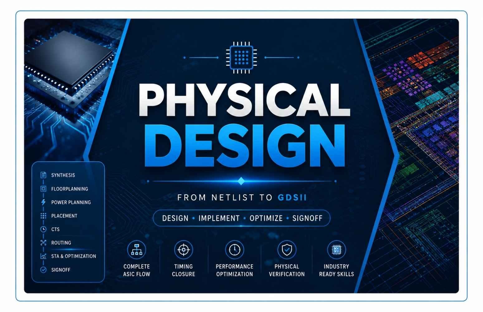
Learn how a synthesized digital design is transformed into a physical chip layout through floorplanning, power planning, placement, clock tree synthesis, routing, timing analysis and physical verification.
SkillChip’s Physical Design course is designed for ECE and electronics students and graduates who want to develop practical knowledge of the VLSI backend design flow and prepare for careers in the semiconductor industry.
Learn the Technology Behind Modern Chip Implementation
Physical Design is the backend stage of ASIC development where a logical design is transformed into a physical layout that can ultimately be manufactured as a semiconductor chip.
This process involves making critical decisions about where cells and macros are placed, how power is distributed, how clocks are delivered, how signals are routed and whether the design meets timing and physical design requirements.
Our VLSI Physical Design course takes you through this journey step by step—from the fundamentals of ASIC implementation to advanced concepts such as timing closure, congestion optimization, ECOs and physical signoff.
The curriculum is structured to help learners understand not only what happens at each stage, but also why it happens and how Physical Design engineers analyze and solve problems during implementation.
These areas closely reflect the core stages found in current industry-oriented Physical Design curricula.
Understand the complete ASIC backend journey and see how every Physical Design stage connects to the next — from RTL / Netlist to final GDSII signoff.
The starting point of the physical design journey, where the RTL or synthesized netlist represents the logical design of the chip.
Follow the journey: Each stage builds on the previous one, taking the design closer to a fabrication-ready semiconductor layout.
A structured learning path covering the complete RTL-to-GDSII journey — from semiconductor fundamentals and synthesis to timing closure, ECO and final signoff.
Physical Design becomes easier to understand when individual concepts are connected to an actual implementation flow.
Key stages covered through practical learning
The practical sequence connects individual Physical Design concepts with the broader ASIC implementation, timing closure, verification and signoff process.
Develop practical familiarity with the tools and technologies commonly associated with synthesis, physical implementation, timing analysis and physical verification.
Technologies relevant to ASIC backend workflows
The tools displayed here should reflect the software actually available in the SkillChip training environment. Update this list based on the tools and licenses provided to learners.
This course is designed for learners who want to develop a structured understanding of ASIC Physical Design and build a foundation for VLSI backend roles.
A structured starting point for learners who want to connect their electronics and VLSI knowledge with ASIC Physical Design.
A chip can have logically correct RTL and still face problems during physical implementation. Physical Design engineers solve the challenges involved in turning a logical design into a physical implementation.
Physical Design works across multiple engineering constraints to transform the gate-level design into a physical implementation ready for verification and manufacturing.
The goal is to transform the logical design into a physical implementation that satisfies the required design and manufacturing constraints. That's why Physical Design sits at the heart of the VLSI backend implementation process.
Ask Us Anything, We’re Here to Help
Have any kind of queries, find the answers in below Physical Design FAQs
A VLSI Physical Design course teaches the backend implementation of an ASIC, covering stages such as synthesis, floorplanning, power planning, placement, clock tree synthesis, routing, static timing analysis and physical verification.
ECE, EEE, electronics and related engineering students and graduates can learn Physical Design. It is particularly relevant for learners interested in building a career in the semiconductor and VLSI industry.
Yes. ECE students with a basic understanding of digital electronics can build their knowledge progressively through a structured Physical Design curriculum.
No prior professional Physical Design experience is necessary to start learning the fundamentals. Basic digital electronics knowledge is recommended.
The curriculum covers ASIC design flow, synthesis, SDC constraints, floorplanning, power planning, placement, CTS, routing, STA, timing closure, ECOs and physical verification.
Yes. STA is an important part of Physical Design. The curriculum covers timing paths, setup and hold analysis, slack, constraints, timing reports and timing optimization.